

Numbers
In digital circuits, numbers are implemented in binary notation and all mathematical operations - addition, subtraction, comparison, multiplication, division or modulo - are performed by manipulating bits.
Example: Even or Odd Number
We will design a circuit that receives a 4-bit input number and activates the output (
A binary number is even if its least significant bit (LSB) has the value 0.
We define the input variable:
The least significant bit is
The output is a single bit:
if the number is even. if the number is odd.
Partial example table (the complete one would have 16 rows):
| Number in decimal | Parity | |||
|---|---|---|---|---|
| 0000 | 0 | 0 | Even | 1 |
| 0001 | 1 | 1 | Odd | 0 |
| 0010 | 2 | 0 | Even | 1 |
| 0011 | 3 | 1 | Odd | 0 |
| 1110 | 14 | 0 | Even | 1 |
| 1111 | 15 | 1 | Odd | 0 |
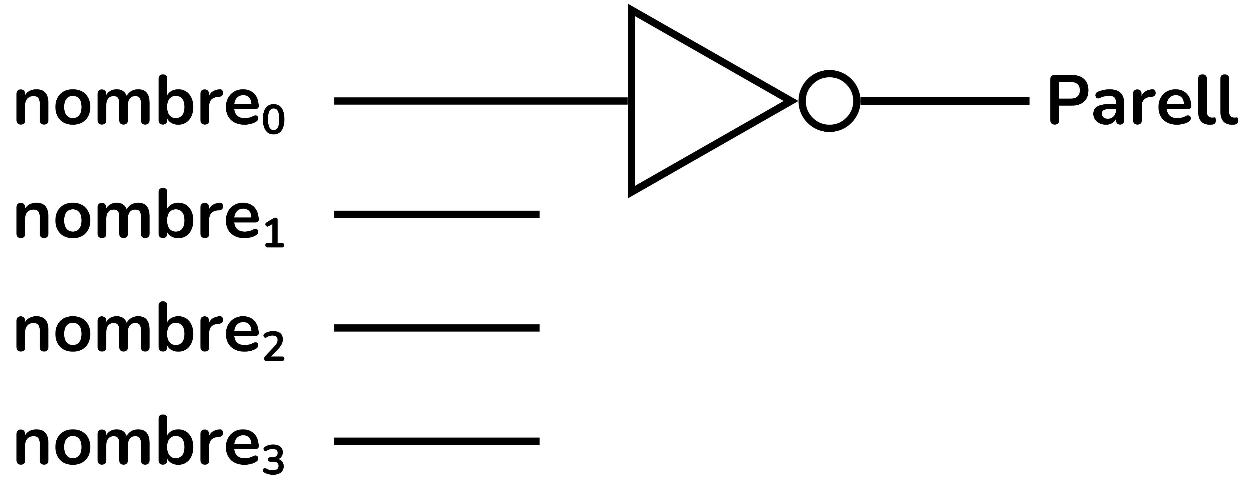
Building the circuit is fairly straightforward; the output Parell must be activated (value 1) if and only if nombre[0] has the value 0, regardless of the value of the remaining bits of nombre.
Therefore, the output is the negation of
Thus, only a single NOT gate is required.
Example: Modulo 7 of a 4-bit number
We will design a circuit that computes the modulo 7 of a binary number
A 4-bit number
The remainders after dividing a number by 7 can take values from 0 to 6. To represent the result of the operation, a 3-bit number will suffice, which can take values from 000 to 111 (0 to 7 in decimal).
The first step in designing this circuit is to create the complete truth table that relates each 4-bit input
| 0 | 0000 | 0 | 000 |
| 1 | 0001 | 1 | 001 |
| 2 | 0010 | 2 | 010 |
| 3 | 0011 | 3 | 011 |
| 4 | 0100 | 4 | 100 |
| 5 | 0101 | 5 | 101 |
| 6 | 0110 | 6 | 110 |
| 7 | 0111 | 0 | 000 |
| 8 | 1000 | 1 | 001 |
| 9 | 1001 | 2 | 010 |
| 10 | 1010 | 3 | 011 |
| 11 | 1011 | 4 | 100 |
| 12 | 1100 | 5 | 101 |
| 13 | 1101 | 6 | 110 |
| 14 | 1110 | 0 | 000 |
| 15 | 1111 | 1 | 001 |
For each output (
Output
We construct the Karnaugh map for the 4 input variables for the output residue_0 and identify 3 groups.
n1 n0 n3 n2 | 00 | 01 | 11 | 10 |
|---|---|---|---|---|
| 00 | 0 | 1 | 1 | 0 |
| 01 | 0 | 1 | 1 | 0 |
| 11 | 0 | 1 | 0 | 0 |
| 10 | 0 | 1 | 1 | 0 |
n1 n0 n3 n2 | 00 | 01 | 11 | 10 |
|---|---|---|---|---|
| 00 | 0 | 1 | 1 | 0 |
| 01 | 0 | 1 | 1 | 0 |
| 11 | 0 | 1 | 0 | 0 |
| 10 | 0 | 1 | 1 | 0 |
The simplified Boolean expression for residue_0 will have 3 terms:
Output
We build the Karnaugh map for the 4 input variables for the output residue_1 and identify 2 groups.
n1 n0 n3 n2 | 00 | 01 | 11 | 10 |
|---|---|---|---|---|
| 00 | 0 | 0 | 1 | 1 |
| 01 | 0 | 0 | 1 | 1 |
| 11 | 0 | 0 | 0 | 0 |
| 10 | 0 | 0 | 1 | 1 |
n1 n0 n3 n2 | 00 | 01 | 11 | 10 |
|---|---|---|---|---|
| 00 | 0 | 0 | 1 | 1 |
| 01 | 0 | 0 | 1 | 1 |
| 11 | 0 | 0 | 0 | 0 |
| 10 | 0 | 1 | 1 | 0 |
Aquesta expressió booleana simplified for residue_1 tindrà 2 termes:
Output
For the output residue_2, identify 2 groups on its Karnaugh map.
n1 n0 n3 n2 | 00 | 01 | 11 | 10 |
|---|---|---|---|---|
| 00 | 0 | 0 | 0 | 0 |
| 01 | 1 | 1 | 1 | 1 |
| 11 | 1 | 1 | 0 | 0 |
| 10 | 0 | 0 | 0 | 0 |
n1 n0 n3 n2 | 00 | 01 | 11 | 10 |
|---|---|---|---|---|
| 00 | 0 | 0 | 0 | 0 |
| 01 | 1 | 1 | 1 | 1 |
| 11 | 1 | 1 | 0 | 0 |
| 10 | 0 | 0 | 1 | 1 |
Thus, the simplified Boolean expression for residue_2 will have 2 terms:
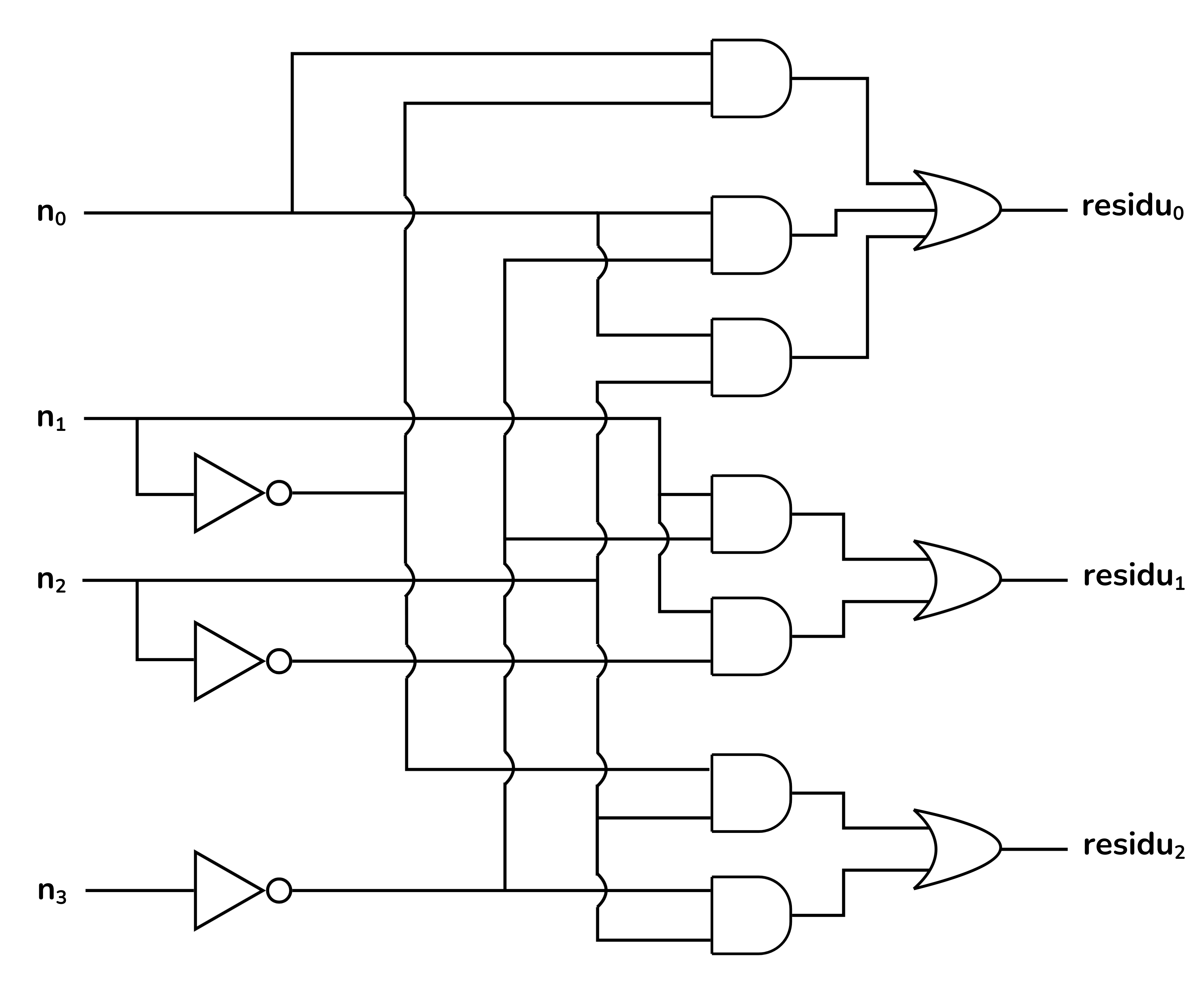
From these three expressions we can use logic gates to create the digital circuit that will implement the function
Exercises on Jutge.org: [Introduction to Digital Circuit Design]
Remember that to access the exercises and for the Jutge judge to evaluate your solutions you must be enrolled in the course. You will find all the instructions here.



Xavier Casas, Francesc Madrid
Lliçons.jutge.org
© Universitat Politècnica de Catalunya, 2026